
Building a TIS100 Node for an FPGA
It’s been awhile since I used an FPGA toolchain, so I was looking for a good project to use as a refresher.
As mentioned before in the Exapunks article, I’m a big fan of the Zackatronics games. I thought implementing one of their toy processors would be a good balance of challenge, while not being too crazy. I decided to go with the architecture used in the game TIS100.
Since they were the tools I was most comfortable with, I did my development on Windows using the Xilinx Vitis + Vivado toolchain. The Vitis name is actually new since I last used the Xilinx tools, but the basic workflow hadn’t changed much. For reference this work was done with version 2019.2.
Another high level overview of this project can be found in the README on Github: https://github.com/axlan/tis100-fpga
Design Process
The first step was learning all the details of the TIS100 nodes. My main resource was the links in https://tis100.complexity.nl/links.html. It had pretty much all the resources I’d need along with source for a bunch of emulators. I also spent some time poking around in the game itself to remind myself of the behavior.
I tried to go about this using test driven design. For each piece of functionality, I’d write a python script that would generate the stimuli to feed into a component, and the expected output. Then I’d create the component in Verilog (a hardware description language), and create something called a test bench to run the unit test for the component. This unit test was performed by using the simulator built into Vivado. I used the behavioral simulation to just check to make sure my logic was correct.
Node components
My design evolved as I built up the components. Back in college, we did some designs for MIPS. I wanted to make things as simple as possible so I took a gamble that I wouldn’t need to pipeline the processor at all.
From this I decided to break the node into 5 modules source code:
- alu (arithmetic logic unit) - Module to perform arithmetic operations
- dir_manager - Module to control communication with adjacent nodes
- instr_ram - Module to read/write instructions from ram and control program counter jumps
- op_decode - Module for decoding binary instructions
- registers - Module to control storing values to BAK and ACC registers
Binary instructions
Eventually I got to the point where I realized I needed to create an instruction set. I did this by working on a compiler and working backwards to figure out the minimal number of bits I’d need to capture all the possible TIS100 programs.
The format is (len in bits):
[4 op][3 src][11 const][3 dst] = 21 bits
- op denotes the type of operation
- src is the source register
- const is a constant immediate value (for example the 5 in
ADD 5) - dst is the destination register
All jump instructions use the const field to give the absolute address to jump to.
See compiler source for more details.
Processor Interface
Once I could start putting these pieces together, I needed to figure out how to interact with them on the FPGA. I went through a couple rounds of refactoring before settling on how to proceed. One particularly frustrating challenge is that the Xilinx tools do not play well with version control. I had to go through several scripts to try to get a set of project files that were reproducible.
Since I had a development board for it, I used a MicroZed board as my target platform. This let me run C code on an ARM processor that could directly communicate with my circuit in the FPGA. I did this by making my code a custom IP block. This block is pulled into a block design and connected to the processor by an interface called an AXI bus.
I ended up creating an interface with the following control registers:
- data_stream - write: send data to node up_in bus, read: read data from down_out bus
- irq_status - read only: irq status register bit 0: output_ready bit 1: ready_for_input
- irq_enable - controls which bits in irq_status will trigger the interrupt output
- instruction_write_address - sets an instruction address to write to
- instruction_write_data - writes a new value to the specified instruction address and resets the node
Here’s a video walking through the design, and showing it in action:
Debugging Process
Validating with a Python emulator
I ended up making a Python TIS100 emulator to validate the integration. This was especially useful when I had to check the results and timing of inter-node communication. I ended up creating mine from scratch so it would be easier to work into my testing workflow.
I was able to compile a TIS100 instruction file, and run the results through both the emulator, and simulator to verify the result. The emulator source can be found here
Giving up on ANY and LAST
Implementing the node components went fairly smoothly. Only the dir_manager was particularly tricky. I decided to give up on supported the ANY and LAST virtual ports since I didn’t see a way of including them without a big jump up in complexity. The only approach I came up with would be to number the nodes from 1 to 4 so that each node would have neighbors numbered 1, 2, 3, and 4. Something like the grid below:
| 3 | 4 | 1 | 2 | 3 |
| 3 | 2 | 1 | 4 | 3 |
| 1 | 2 | 3 | 4 | 1 |
| 1 | 4 | 3 | 2 | 1 |
| 3 | 4 | 1 | 2 | 3 |
Each TIS100 instruction cycle would take at least 4 FPGA clock cycles to check the reads. All the 1 numbered nodes would check first first, then the 2 nodes and so on. This way there wouldn’t be any contention.
However, I wasn’t really interested in implementing this complexity, and I thought it was a less “true” implementation of this processor design, where it actually takes the same cycles as the game implementation.
Finding a well hidden simple mistake
When I first put all the pieces together, I was disappointed to find that the live hardware wasn’t giving the correct results. Debugging an FPGA can be very tricky mostly because it is very hard to observe it’s internal state. I used the Xilinx debug tool called ChipScope, to compile in a scope to capture some of the signals based on a trigger condition. Like software, the compilation process optimizes away a lot of the values, so I had to relearn how to examine the schematics to find suitable points to record.
In addition, the FPGA and ARM need to be configured to run the node in order for me to capture the failing operation, but both the configuration and the ChipScope capture use the same JTAG interface. I decided to use a physical push button on development board so I could set things up, then switch to using ChipScope with the JTAG and press the button when I was ready to trigger the event to capture.
Here’s what I captured:
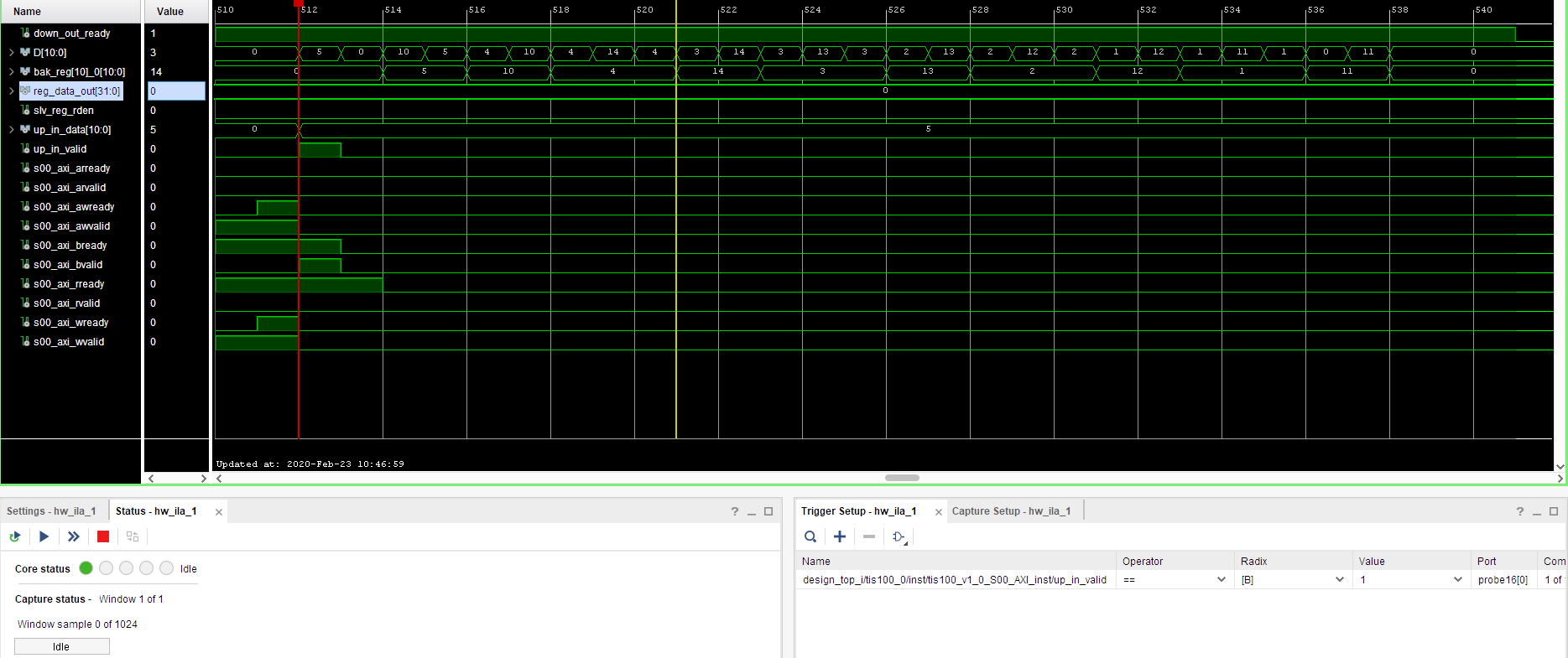
This capture is showing the node attempt to execute the following code:
1
2
3
4
5
6
7
8
MOV UP ACC
L1: SWP
ADD 10
SWP
SUB 1
JNZ L1
SWP
MOV ACC DOWN
While it looks like the data was getting into the node correctly, it starts storing the wrong value a few instructions in. You can see it load 5 as its input, swap, add 10, swap, and subtract 1. But after that it seems to store the wrong value.
At first I thought this might be due to a timing issue. One of the main complications of FPGA design over software is that you need to account for the delay caused by running singles through logic gates, and over long wires.
To test this I finally decided to run some timing simulations. These simulations try to account for these delays, and are based on the actual signals that are used in the FPGA. This makes interpreting them much harder, since they don’t necessarily correspond with their source code names. I was eventually able to make my life easier by turning some of these optimizations off.
I was able to reproduce the behavior in my timing simulation:
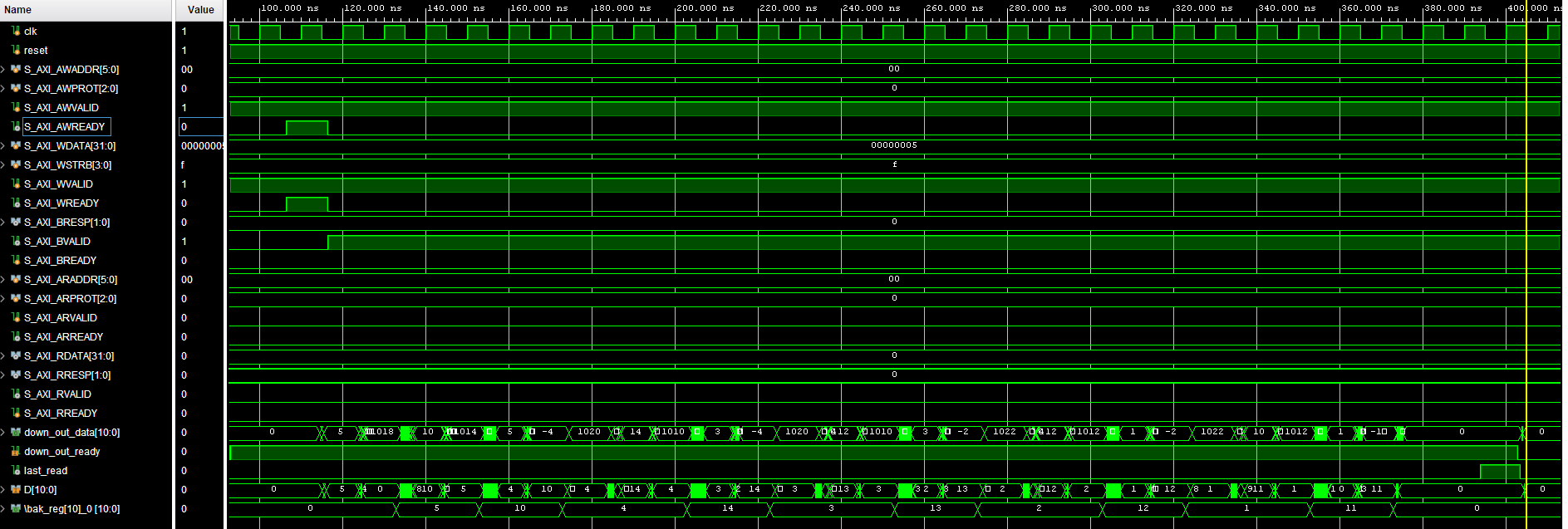
This let me get a lot more context on what was happening and dig into each connection to see where things were going wrong. The op_decode module determined what the register module should do this cycle with the following logic:
1
2
3
4
5
6
7
assign registers_instr = (op == OP_MOV
        || op == OP_ADD
        || op == OP_SUB
        || op == OP_NEG) ? INSTR_REG_WRITE :
    (op == OP_SWP) ? INSTR_REG_SWP :
    (op == OP_SAV) ? INSTR_REG_SAV :
    2'bx;
This code assigns the wire registers_instr which controls the registers action. It checks the current command and sets registers_instr to INSTR_REG_WRITE, INSTR_REG_SWP, INSTR_REG_SAV, or 2’bx. 2’bx is a placeholder that sets the value to unknown. It was only chance that this worked in simulation, since it should set the wire under those conditions to INSTR_REG_READ. Somehow the behavioral simulation still worked with this output. I must have made this mistake early on, and didn’t update it to the correct value as I was writing the module.
It was a super easy fix once I realized it, but the exercise was a good chance to refresh myself on the FPGA debug process. It shows the blind spot in my behavioral test driven development process. In the future I should probably try at least one timing simulation integration test to try to catch similar errors.