
Location Display Map with PCB Art
I used a free PCB sponsorship as an excuse to build the biggest board I’ve ever designed. I turned it into a living map of my family.
To my great surprise, PCBWay reached out and offered to cover the manufacturing costs for a board in exchange for a mention on this hallowed blog. While I’ve avoided monetizing this blog in any way (including removing analytics), it turns out I’m not incorruptible when presented with an excuse to design a giant PCB. As you’ll probably be able to tell from the rest of the article, PCBWay had no involvement itself in the project or write up beyond agreeing to manufacture it.
I like using constraints as inspiration, and I wanted to build something that took advantage of the PCB medium itself.
All of the designs and source code for this project can be found at: https://github.com/axlan/pcb-map
While I don’t think I rushed the project, I did try to move faster than usual. With a new baby in the house, project time could sometimes feel borrowed, either from my family or from my already limited sleep. Still, making things is important to me, and in its own way, this project became a form of self-care. In some places that tradeoff worked out well. In others, not so much. See the Improvements section for the consequences of moving a little too quickly.
UPDATE
It was interesting to see the comments on Hackaday focused on the privacy implications of the project. The location data comes from Google’s built-in location sharing feature, which is opt-in, gives periodic reminders while enabled, and is easy to turn off. The PCB map itself hangs in a shared space and, given its relatively low resolution, is far less useful for stalking someone than simply opening Google Maps on a phone.
That said, I completely understand the reaction. We’ve largely normalized being tracked digitally, but there’s something more visceral about seeing that tracking represented physically in the real world instead of abstractly existing on a server somewhere.
Previous PCB Designs
As a kid doing hacky electronics projects, having a custom PCB made felt like an unimaginable luxury. It was exciting when I got to college and was able to get a discount on manufacturing a board for my final project (a persistence of vision display). Even then, I still ended up making the second of the two boards the project needed myself using toner transfer and ferric acid copper etching.
More recently, I made a little game handheld that could play snake or track the state of a Magic the Gathering game. Here, I had fun adding some decorative flourishes and got to practicing using a modern KiCad version.
Brainstorming
While I knew I wanted the PCB itself to be the centerpiece, I went through a long list of ideas before settling on one.
I spent some time specifically looking at other PCB art projects. There’s a lot of beautiful stuff out there. One site I found particularly interesting was Boldport. In particular, https://boldport.com/blog/2013/09/the-lifegame.html reminded of my recent wedding project. They actually have a whole design tool for PCB art https://github.com/boldport/pcbmode which I looked into. Unfortunately, it seems like the site and the tool haven’t really been active for a few years.
Another PCB art project that inspired me was https://chaijiaxun.com/blog/pcb-metro-map-build-log/. The author created meticulous transit maps as PCBs with light animations.
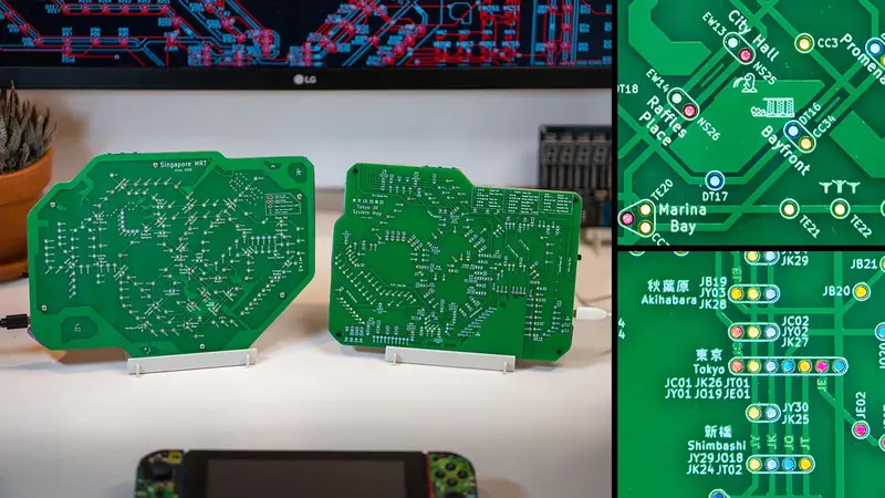
These two projects both dealt with illuminating PCB’s from the back. I used them as points of reference as I settled on my own design. The creator of the PCB Metro Map Chai Jia Xun in particular spent a lot of effort on perfecting his approach. He ended up shining light through the via holes in the board, coloring them with paper, and using a printed mask to avoid light leaking between holes.
With my prior art research done, I focused on coming up with my own design.
My default instinct for an interesting display project is always to turn it into a clock. I explored designs that combined static PCB artwork with dynamic elements like LEDs, LCDs, e-ink panels, and seven-segment displays. I considered building a traditional clock, a calendar, and even an orrery. But the more I explored those ideas, the more conventional they felt. I wanted something stranger and more personal.
In the end, the most interesting direction was a display that reflected the daily rhythms of my family in real time.
Of course, this takes inspiration from the “Weasley family clock” from Harry potter. Many people have made beautiful projects recreating the clock, and a few that incorporate the electronics to make it function like in the books as well. To put my own spin on it, I decided to combine the idea with the PCB Metro Map to make the display a map.
High Level Design
First, I had to settle a few basic layout questions:
- What geographic area should the map cover?
- Should the map be contiguous, or split into multiple regions?
- Should it include zoomed-in sections?
- How would I indicate which family member was which? Would I need RGB LEDs to create distinct colors?
I also considered an approach where a row of circles along the bottom of the board would call out points of interest like home or school, with lines connecting them back to their locations on the map.
There was also the question of how to light the board. I could either place LEDs on top of the PCB or mount them underneath it. LEDs mounted below the board would need some way for the light to shine through. Either holes through the PCB or regions without copper. The PCB Metro Map project meticulously tested the lighting and tempted me to take one of the more complicated approaches. Chai Jia Xun ended up shining light through via holes in the PCB, coloring them with paper, and using a printed mask to prevent light from leaking between holes.
As I explored lighting options, I also started thinking about the assembly process. I’ve built several projects that required soldering dozens of RGB LEDs (like the Icosahedron Globe and the Pixel Wreath) and it can be both tedious and finicky. Over time, I’ve learned that starting with the right off-the-shelf LED hardware can save an enormous amount of effort.
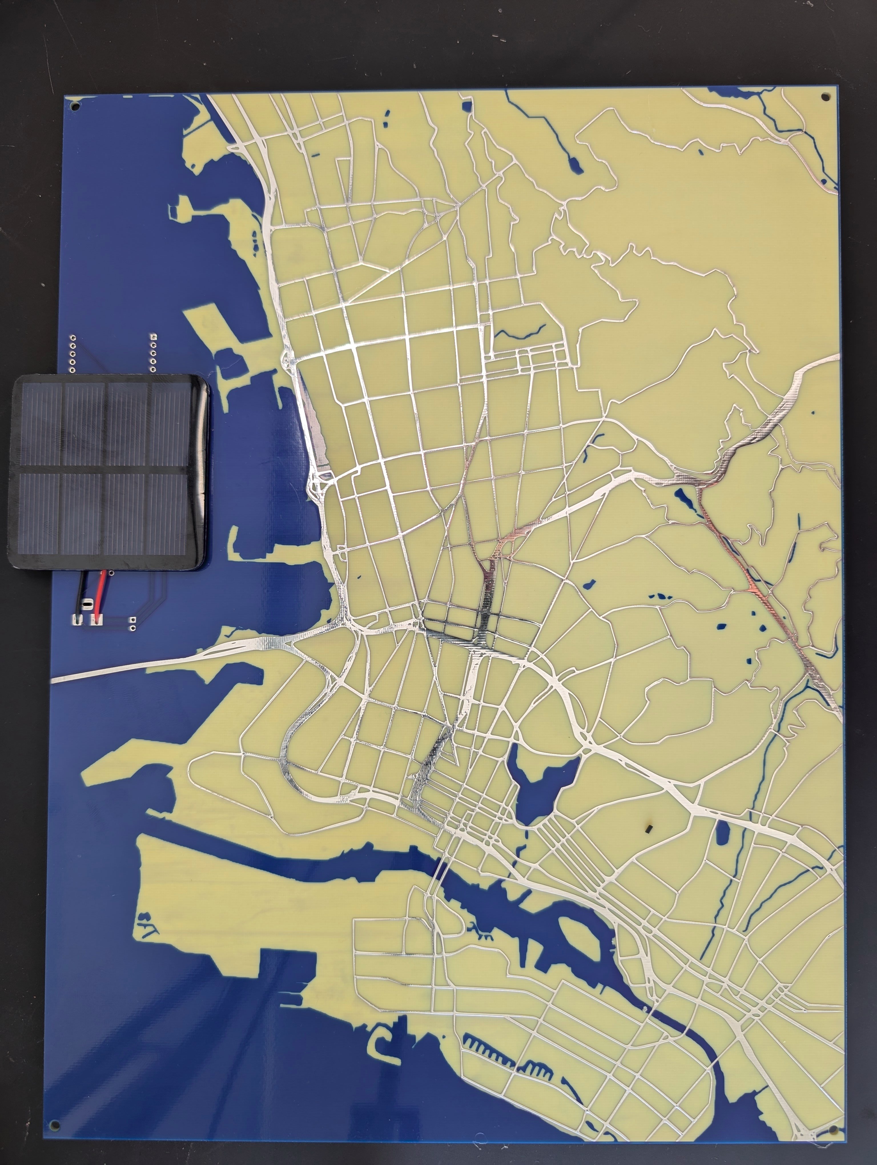
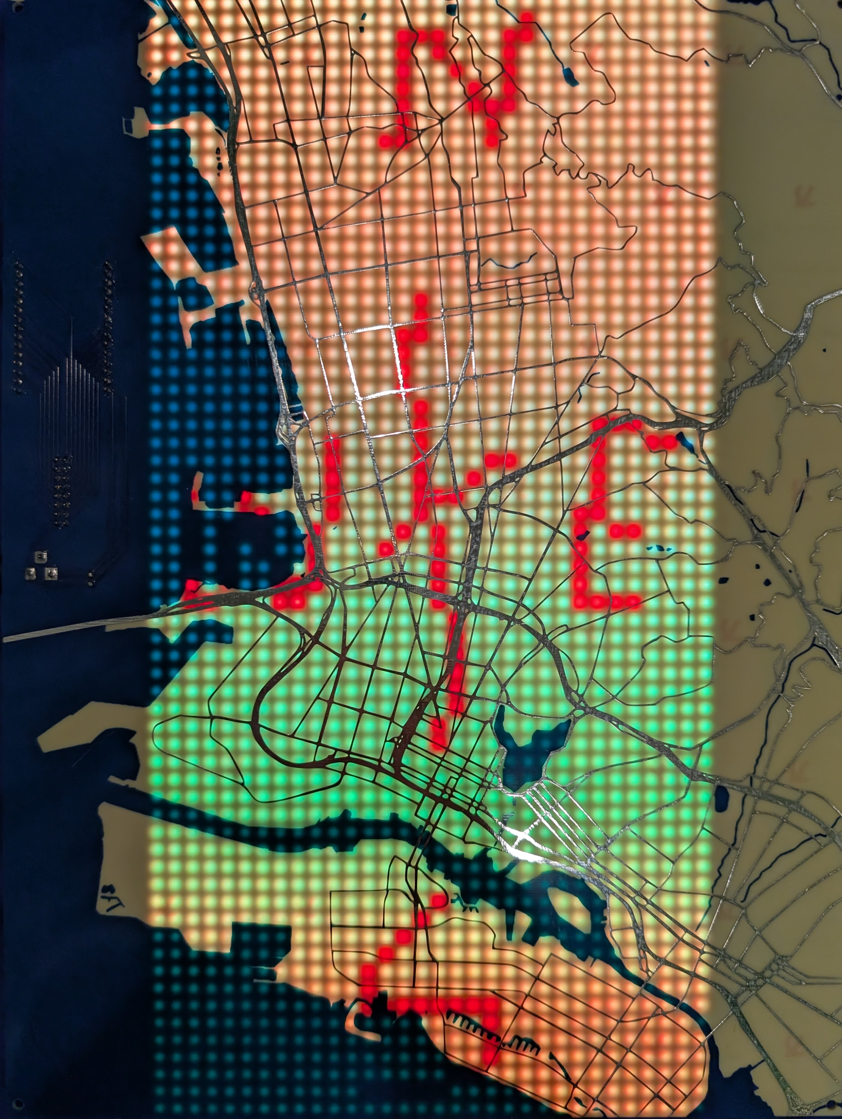
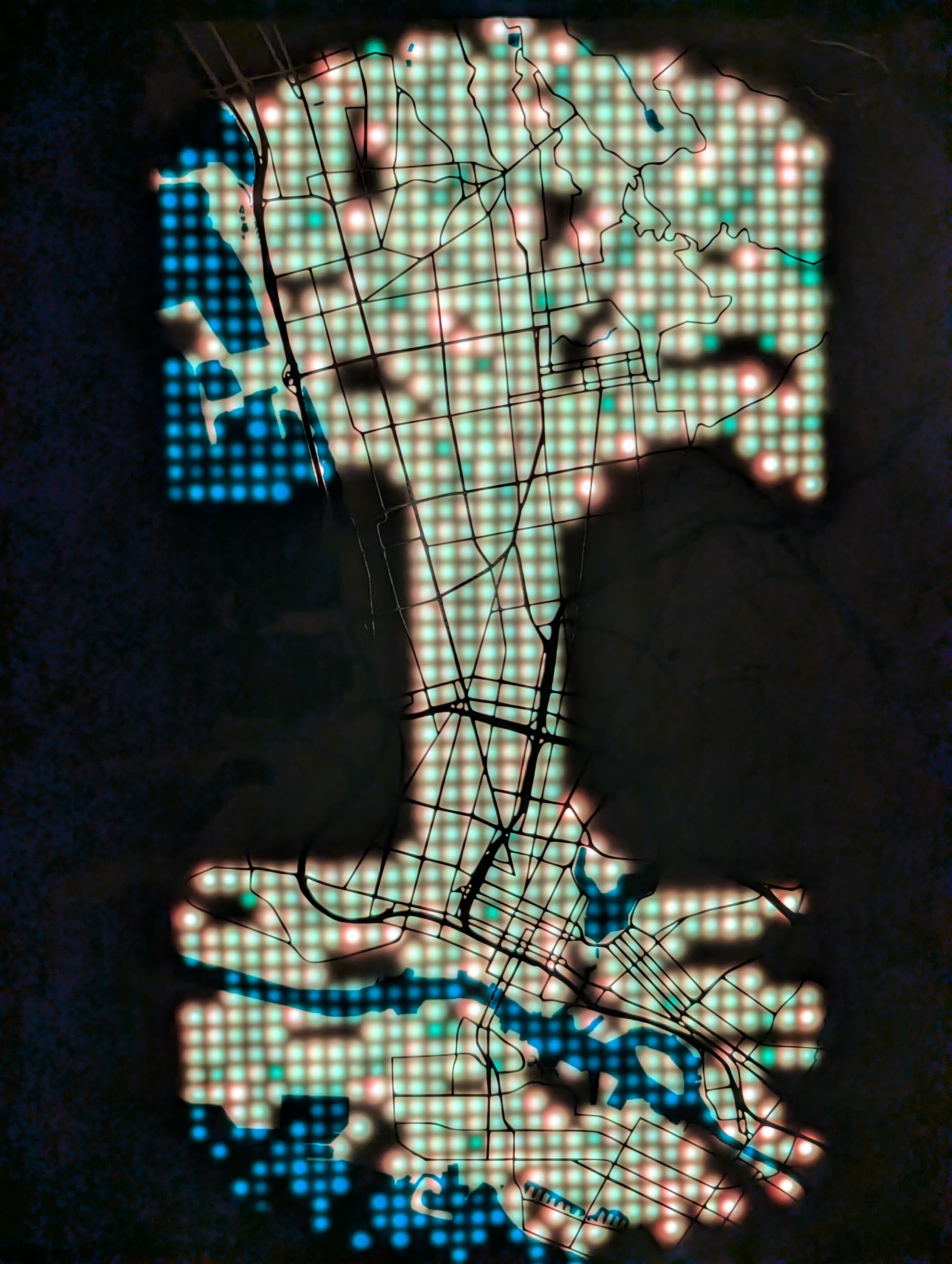
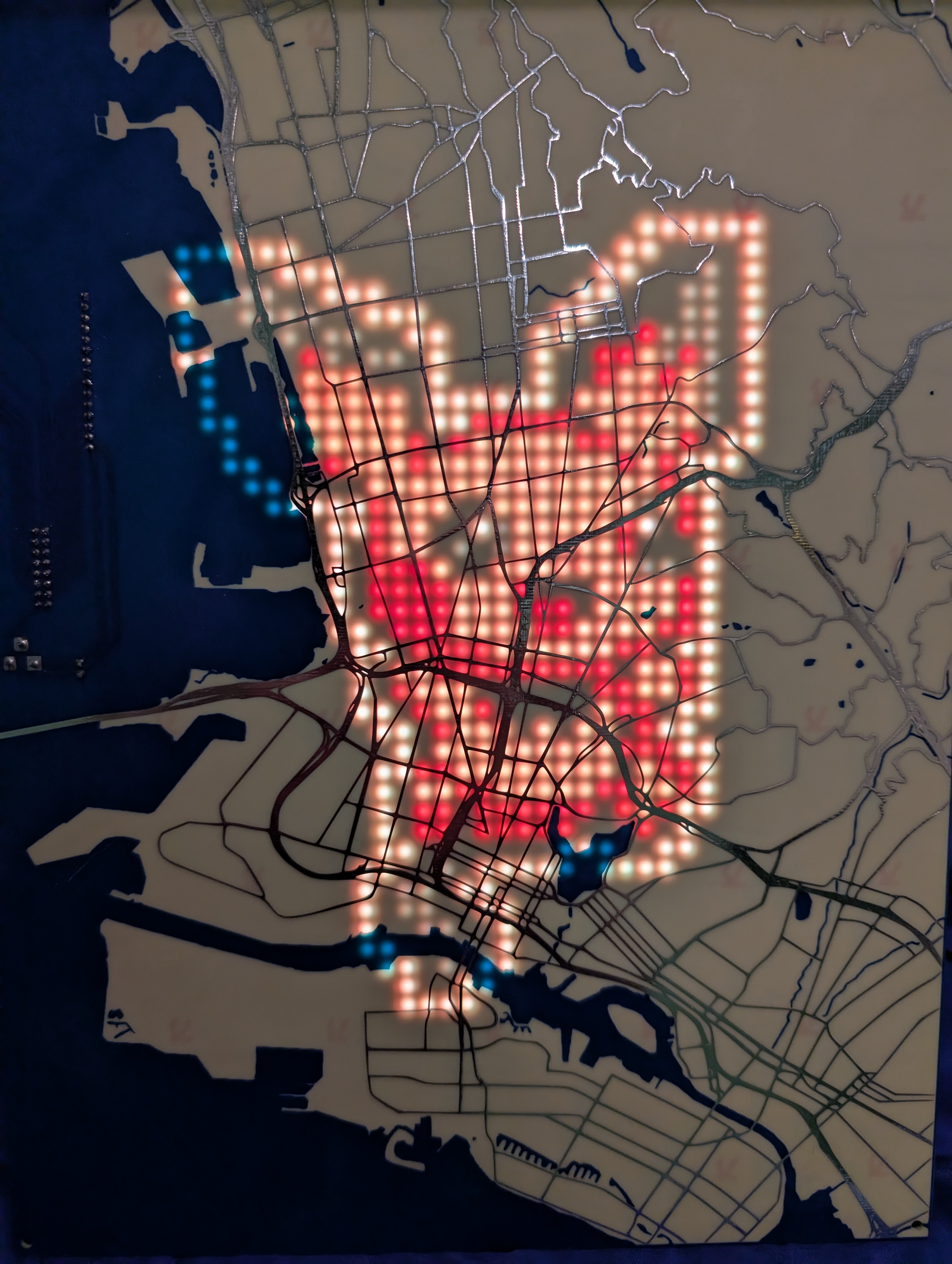
Since the goal was ultimately to illuminate points on a map, what I really needed was a dense LED grid. It turns out there are plenty of inexpensive RGB LED matrix panels available, and I found 64x32 panels selling for around $30. That was dramatically cheaper (and far less work) than populating the board with individual RGB LEDs.
Once I committed to using an LED matrix, the rest of the design started to come together. I decided to make the largest PCB I could reasonably pair with a 64x32 panel. I included the surrounding hills and water to create a more balanced, square composition, while centering the LED panel on the areas we actually travel through.
After ordering a panel, I found that it looked fine shining through a test PCB without copper or solder mask, which simplified the design considerably.
As usual, I ended up using an ESP32 development board to drive the display.
Making the PCB
PCB Design
All the design files can be found at https://github.com/axlan/pcb-map/tree/master/design.
I usually try to make my projects as automated and repeatable as possible (often to a fault). I’ll spend far more time building tooling and infrastructure than it would take to do a one-off task manually. For the map artwork, though, I gave myself permission to just wing it and focus on getting the design finished as directly as possible.
I initially considered using the Boldport PCBmodE tool, but it appeared to be unmaintained and seemed like it would come with a steep learning curve. Instead, I decided to try the image converter now built into KiCad.
Since the KiCad converter only works with bitmap images (JPGs, PNGs, and similar formats), I didn’t need to worry about building everything as vector artwork.
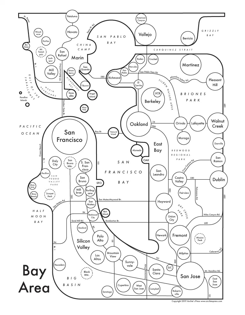
I also explored more abstract map styles, including this design from Archie’s Press:
In the end, though, I decided to stick with a normal geographic map.
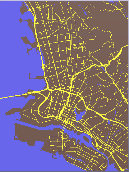
I was surprised by how difficult it was to find a good source for the map imagery. If I had wanted to be truly meticulous, there are probably mapping APIs that expose the underlying geographic features directly so you can render everything exactly how you want. Instead, I mainly needed an online map tool where labels (road names, points of interest, etc.) could be disabled cleanly.
Eventually, I found Snazzy Maps, which was almost exactly what I was looking for. It provides a JSON-based styling interface with fairly fine-grained control over map appearance. I started from the existing Assassin’s Creed IV style and disabled railroads and local streets.
The site includes an export button, but it only supports images up to 1000x1000 pixels. Instead, I rendered the map at high resolution and captured screenshots manually.
Next I had to decide what map features I wanted to have on which PCB layers.
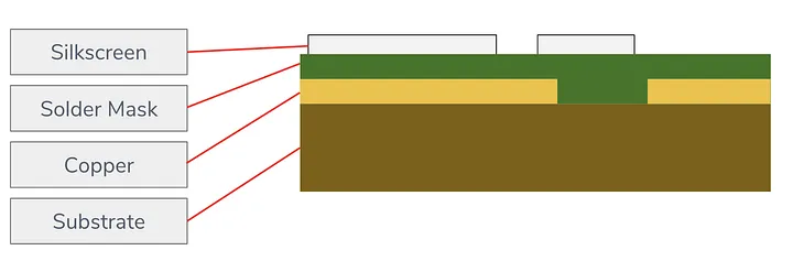
PCBs normally have these layers on both the front and back of the board, though additional copper layers can also be sandwiched internally. Since I planned to shine light through the PCB, I realized I could also use the back-side layers to block or dim light without affecting the visible front surface. Vias (the plated holes that connect copper layers together) could even be used to channel light directly through the board.
In the end, I decided to keep things simple:
- Solder mask for water
- Exposed copper for streets
- Bare PCB substrate for land
To make the board translucent, I removed the copper and solder mask from the entire back side of the PCB. Once I started adding electronics, though, I limited this treatment to the land areas so that I could still place conventional components in the “water” regions.
At that point, I just needed to generate images for each PCB layer I wanted to import into KiCad. Here was the process I ended up using:
- Using Snazzy Maps, I captured a screenshot of the region I wanted to use for the map.
- Since I had decided on a final board size of 240x320 mm, I cropped the image to match the correct aspect ratio.
- I created a reference layer with a 160x320 mm rectangle to verify that the LED matrix panel would fully cover the parts of the map I wanted illuminated.
- Using GIMP, I used the “select by color” tool to separate the image into independent layers for water, land+roads, and roads. I made each layer a solid opaque color.
- The road layer ended up looking heavily pixelated and didn’t import cleanly into the KiCad image converter. To fix this, I copied the roads image into Inkscape and used the “trace bitmap” feature to generate a smoothed vector version of the roads. I then re-exported this at a higher resolution and brought it back into GIMP to create cleaner road geometry.
- I exported PNG images for both the land+roads layer and the roads layer. I also created a horizontally flipped version of the land+roads image for use on the back side of the PCB.
-
Using the KiCad image converter, I imported the PNGs into the PCB design at a final scale of 240x320 mm:
- The roads became a top-side copper layer.
- The land+roads image became a top-side solder mask layer.
- The flipped land+roads image became a bottom-side solder mask layer.
At that point, I had a PCB file containing the complete map artwork.
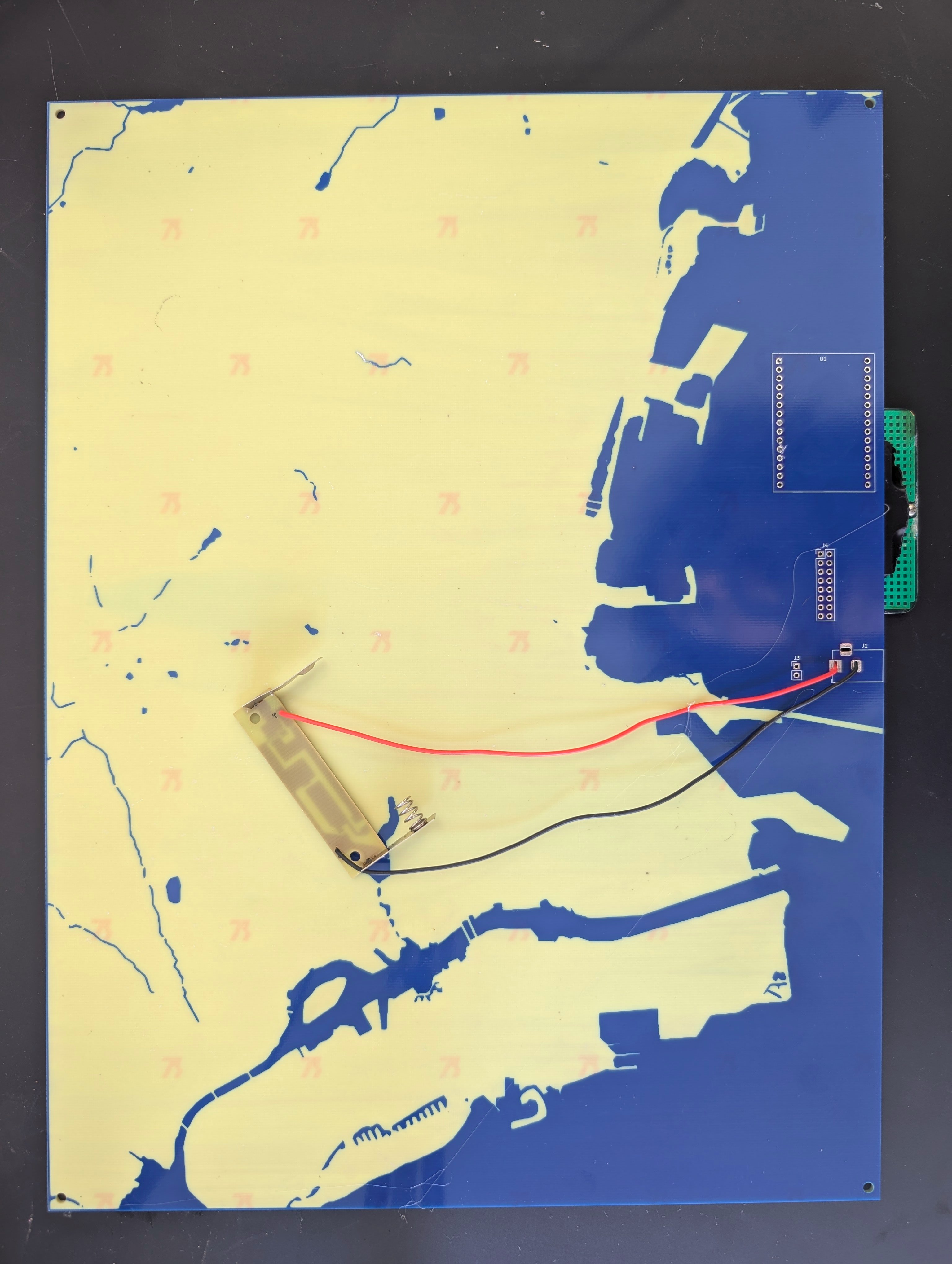
Separately, I created another KiCad project for the actual electronics: the ESP32 development board, LED matrix interface, and power connectors. After verifying the footprints and laying out the PCB connections, I copied the completed electronics layout into the map PCB project.
At one point I considered trying to keep the board single-sided, so I intentionally selected ESP32 GPIO pins that minimized routing complexity and avoided needing additional copper layers.
When I finally ran the design rule checker (DRC), I discovered a few clearance violations near the board edges, so I added roughly half a millimeter of additional margin around the design. It also had issues with the single sided board, so I left it two sided.
One feature I especially appreciated during this process was KiCad’s 3D PCB viewer, which made it easy to preview how the finished board would actually look before sending it off for manufacturing.
PCB Manufacturing
I was curious how PCBWay would react to a giant decorative PCB, so I was pretty eager to get the design into their system and see what happened.
Their upload and ordering interface was straightforward enough. As someone with hobbyist PCB experience I found the process fairly painless. While exploring the manufacturing options, I was briefly tempted by the “hard gold” surface finish. Since my design intentionally exposed a large amount of copper, this would have effectively plated huge portions of the board in gold. Unfortunately, a 30-micron gold finish increased the estimated price from roughly $120 to $572. I also suspected the standard silver finish would probably look better and be less likely to be rejected, so I stuck with that.
One feature I especially appreciated was the ability to preview the board after uploading the design files. It made it easy to sanity-check that the solder mask color and surface finish matched the aesthetic I had in mind.
Once the board was submitted, I had to wait for the design review process. I was curious how this would go, and sure enough, the design was flagged for confirmation:
Hi,
Thanks for your inquiry, here is a question for project No.W1047802AS4C1_map_board.zip
Pls find the attached pic and confirm whether the design is normal or not?
Your timely response would be greatly appreciated!
The attached image was the entire copper layer of the board.
I replied:
This is the intended layout for the top copper layer. The large section is there for appearances only to make the board look like a metal map.
Thanks for double checking.
which got the reply:
Thanks for your reply!
W1047802AS4C1_map_board has been approved now, the PCB price is $126.17, with an estimated lead time of 3–4 days, pls kindly login to check the details and proceed to checkout if everything is in order. :D
Honestly, that felt like the right response. A board that is mostly decorative and only partially functional seems worth double-checking before fabrication, and it was easy enough to clarify the intent. I am curious what the exchange would have looked like if I hadn’t cleaned up the design rule check (DRC) errors before submitting it.
From there, everything went smoothly. PCBWay covered the manufacturing and shipping costs, though I still had to deal with import tariffs. In practice, that just meant FedEx sent me an invoice after delivery for a 31% tariff, plus a $15 processing fee for handling the import payment on my behalf.
Software
From the start, I knew I wanted to keep the panel firmware as simple and generic as possible. Ideally, I could reuse it for other display projects in the future. The device would receive commands over MQTT to drive all dynamic behavior.
This also meant I would need to write a separate host-side application to run on a PC, responsible for querying family locations and translating that data into commands sent to the device.
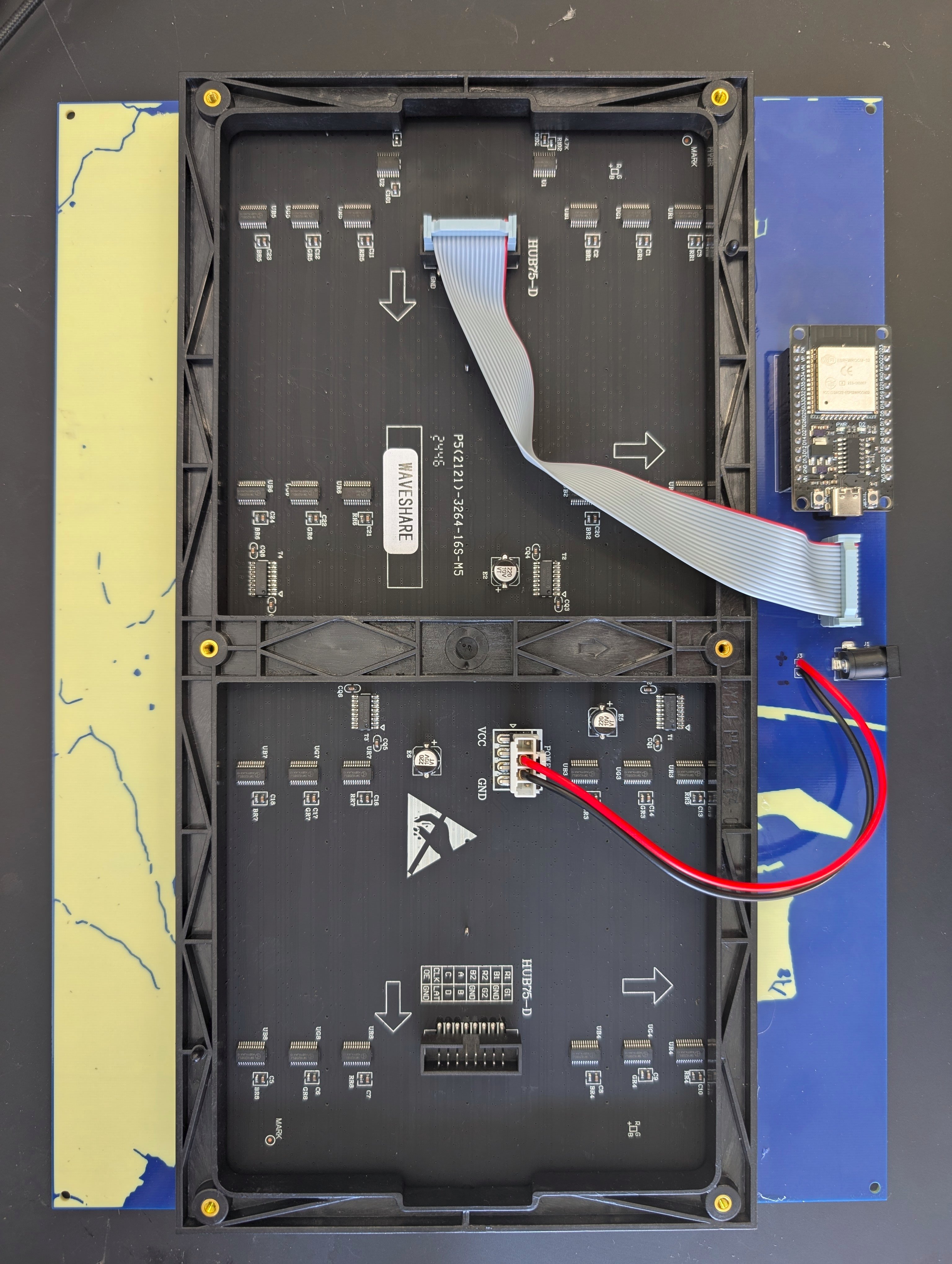
LED Matrix Driver
I bought the LED matrix panel with the hope that controlling it wouldn’t be too much of a pain. From what I can tell, HUB75 is an informal standard that many LED panels implement https://learn.lushaylabs.com/led-panel-hub75/. Since it’s informal, there are many small variations that need to be validated when buying a new model.
The matrix display that this project was tested with is the: Waveshare RGB Full-Color LED Matrix Panel, 5mm Pitch, 64x32 Pixels
It was labeled as P5(2121)-3264-16S-M5 (32x64 1/16 scan) and used the RUC7258D, SM16208SJ, and MW245BC control chips.
Like most embedded projects, finding the “best” library to use is a bit of a pain. It seems many owe their ancestry to the Adafruit graphics library, which has many descendants targeting different platforms and display technologies. After some research, I decided that the https://github.com/mrcodetastic/ESP32-HUB75-MatrixPanel-DMA library seemed to be the most capable and compatible option for the ESP32.
I wired up the panel directly to an ESP32 and tried the example script. The display sort of worked, but everything was slightly glitchy or shifted. Reading the control library README, I tried changing the clock phase setting, and just like that the panel was working correctly.
I did a bit more experimenting and eventually found other display artifacts, but these went away when I switched from jumper cables to my custom PCB. As it turns out, they’re not kidding when they say these boards are sensitive to needing a beefy power supply and short cables. The signal integrity issues might also be partly due to the panel expecting 5V signals while the ESP32 outputs 3.3V.
When my custom PCB arrived, I was delighted that the connection between the ESP32 and the LED panel worked without issue. It’s not that the layout is particularly complicated, but there’s a lot of room for something to get flipped left/right or top/bottom.
As I developed my application, I found the panel library mostly worked as expected and was pretty solid. When I started having issues with flickering, I enabled the library’s built-in double buffering, which fixed the issue.
With the driver done, I needed to implement the display control interface. I didn’t approach this particularly systematically and mostly just added features as needed. I ended up with two basic ways to draw things on the display.
First, I added an interface for drawing a background image. This is simply sending a bitmap of pixel colors for the whole panel to be statically displayed when nothing else overwrites them. When I started testing this, I realized that the MQTT library I was using had a 256-byte message limit. Since I didn’t want to rely on sending 4 KB (64x32x2 bytes, where 2 bytes per pixel is the RGB565 color scheme) messages, I set up the interface to update the background row by row (128-byte payloads).
I also wanted to support drawing elements that could be updated independently and could have some dynamic behaviors (e.g., pulsing). I created a concept of sprites indexed by a name identifier. The only sprite type I implemented was a pixel sprite that could oscillate between two colors. This also enabled the panel to periodically cycle between sprites sharing the same position, to handle the case where multiple people were at the same address and I wanted both to appear on the map. These sprites could then be updated by future commands referencing their name. There are other sprite types I could have added (such as driving routes) but I decided not to add complexity to the firmware until it was actually needed.
Network Discover Provisioning and Configuration
One of the first things I focused on when building out the firmware was making the network configuration completely reliable. In previous projects, I’d taken a variety of approaches to handling Wi-Fi credentials and MQTT configuration, but this time I wanted something more polished and dependable. I put extra effort into making the setup process stable and user-friendly so that, if I ever wanted to duplicate the project or revisit it in the future, getting it running again would be straightforward.
Setting or updating Wi-Fi credentials requires a side channel to configure the device before it has network access. For the first time, I read through the Espressif provisioning documentation. The Espressif unified provisioning libraries provide a robust way to provision a device over Bluetooth or an ad-hoc Wi-Fi access point. The downside is that the library is fairly complex and requires the host machine to either support Bluetooth or manually connect to the ad-hoc network.
There was also a library called SmartConfig, which uses clever techniques to decode network credentials from the length of encrypted packets by monitoring Wi-Fi traffic. Unfortunately, the documentation suggested this approach may not work consistently across all Wi-Fi drivers.
I ultimately fell back on the WiFiManager library, which I’ve used in previous projects. It still requires manually connecting to an ad-hoc Wi-Fi network, but it creates a captive portal that makes entering credentials straightforward.
To streamline finding the device on the network, I spent some time better understanding how mDNS works. On my Linux system, at least, it let me use the device’s local hostname directly instead of tracking down its assigned IP address.
Once the device is connected and configured, all communication happens over MQTT. This gives me flexibility in choosing between a local or remote broker, handling authentication, and avoiding a lot of lower-level protocol edge cases. Even after the device was online, though, I still needed a way to configure the MQTT host and authentication settings.
I ended up creating a simple UDP command packet format to configure all the parameters used for MQTT authentication. I spent a fair amount of time working through MQTT TLS certificate management before ultimately disabling certificate validation.
Supporting arbitrary brokers securely would have also required transmitting the root certificate through this configuration interface. The added complexity of managing certificates didn’t feel worth the relatively small security benefit of guarding against potential man-in-the-middle attacks for a project at this scale. For a commercial device the calculus would be different. I’d likely target a specific broker, embed the root certificate directly in the firmware, and skip this level of configurability entirely.
I’ll go into the details of how I tried to automate device setup in the Python controls find-devices section.
Simulator
See https://github.com/axlan/pcb-map/tree/master/firmware/simulation for the simulator source code.
While updating the firmware and testing on the device isn’t that painful, I wanted to make development as quick as possible. Since the interface to the display is so basic, it was relatively easy to create a small CMake application to simulate it locally.
I primarily wanted to test the MQTT handling and display logic, so I included the relevant source files from the firmware in my simulator build. To do this I created dummy header files that mocked out any Arduino or driver calls to allow them to compile. I used the SFML graphics library to render my simulated panel overlaid on a transparent map image.
Python Controls
I made two Python tools for interacting with the board. I continue to mostly design Python projects with uv in mind, and here I really tried to get good command-line ergonomics. I used the Typer library for the first time to handle parsing command-line arguments. It worked out well once I learned enough to cover my use cases. One feature I was happy to find was that you can map command-line arguments to environment variables, which makes it easy to set credentials without typing them in each time and without any extra code.
device-setup
The goal of this tool was to eliminate the tedious process of setting up an IoT device. Things like not knowing whether it’s connected to Wi-Fi, or having to log into the router to find it on the network. The states it detects and configures are:

control-server
Once the device is fully configured, further operation is controlled over MQTT. This tool handles that control for various tests and applications.
The main application is display-shared-locations. It loads the user’s and their friends’ positions to draw on the map, and checks calendar events for positions to draw routes to.
For testing purposes I also created a way to specify changing user positions and routes as a JSON file.
One issue I hit while developing this interface is that there’s no great way to access your location data over an API from Google. Google tracks your position and lets you share it with friends through Google Maps, but there’s no official way to access this data outside the app or website. There is a Python library that handles parsing the data, but it requires session cookies, which can be fragile for a long-running server.
I could use a side channel to report positions, but I wanted to avoid requiring my family to run any special software on their phones. Both for simplicity and for privacy.
Position data could also come from other services. If my kids get some sort of non-phone location beacon (like an AirTag), I could potentially integrate that as well, since it would just be an update to the Python server.
Drawing the routes was a bit more involved. I initially used an API from OpenRouteService since its free tier would have covered my usage, but it returned incorrect positions for the test addresses I tried. I switched to the Google Maps routing API, which requires a Google Cloud account but should also be effectively free.
Converting user locations to panel coordinates was a fairly straightforward mapping from latitude/longitude to the panel’s X/Y. Drawing routes was more complex: I receive the route as a series of line segments and need to map these onto the grid. The algorithm I used could almost certainly be improved, but I got something quick and dirty working.
I decided to add route drawing later in the process. Rather than adding a new sprite type for routes, I found it easier to draw them as part of the background image and manage them from the server side.
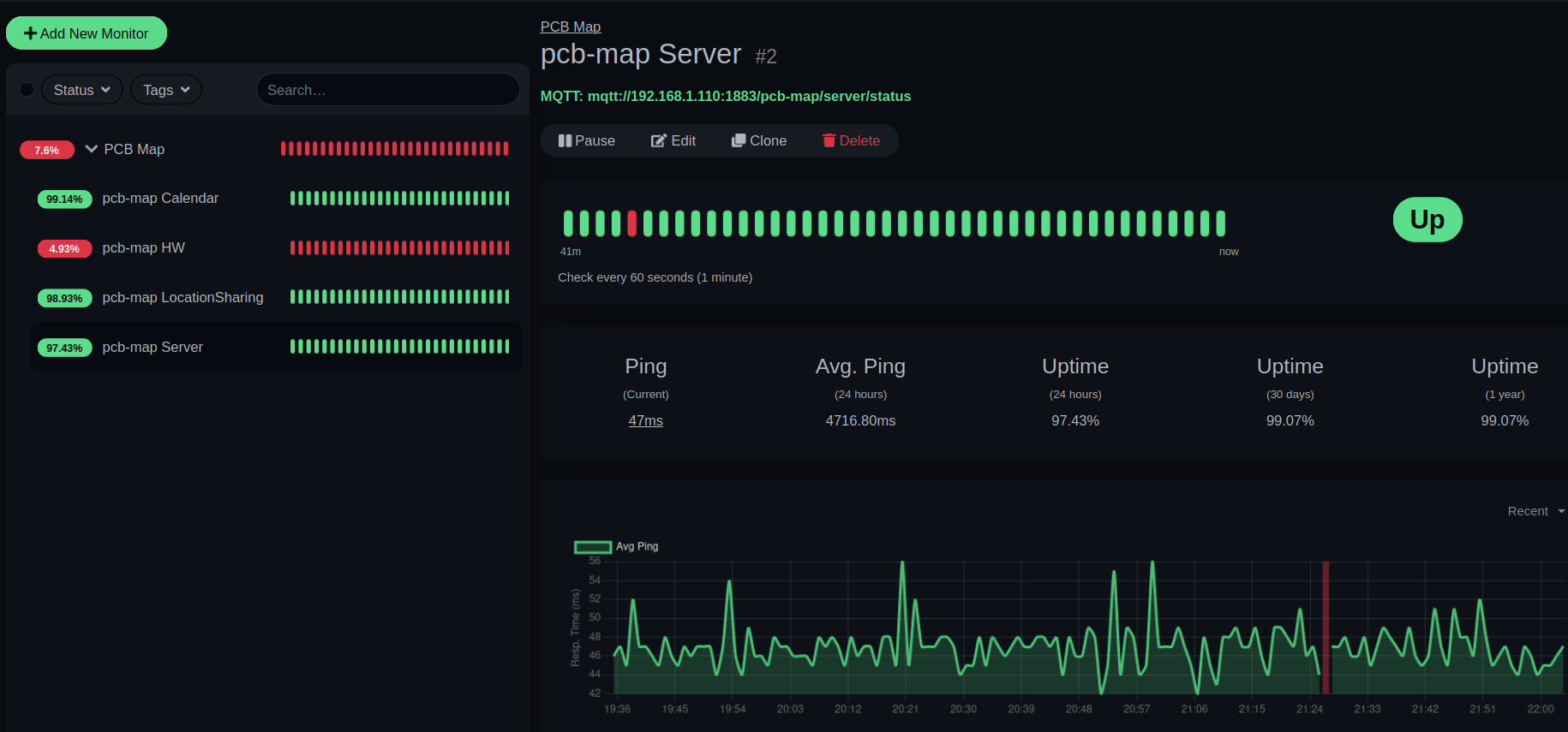
Once I had everything working, I spent some time hardening the application so it would behave more reliably as a long-running server process. I added MQTT status reporting so I could monitor whether the hacky cookie sharing mechanism needed to be refreshed or if some other unexpected failure had occurred.
To run it on my server, I Dockerized the application and wrote scripts to update the authentication credentials as needed. I also set up Uptime Kuma to monitor the service and alert me if anything failed.
Results
I ended up with two complementary projects: the PCB, which is beautiful on its own, and the position display server and firmware for the LED matrix. Using a PCB for the static map is a great aesthetic touch, but the whole thing would be completely functional with a printed paper map instead.
PCB Solar Light
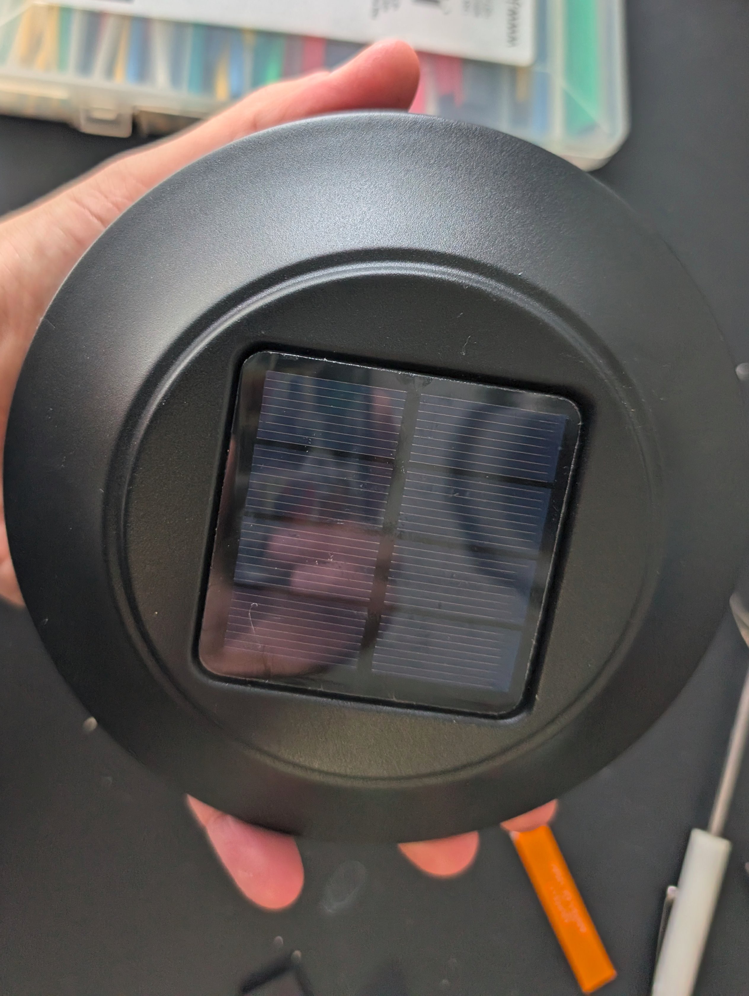
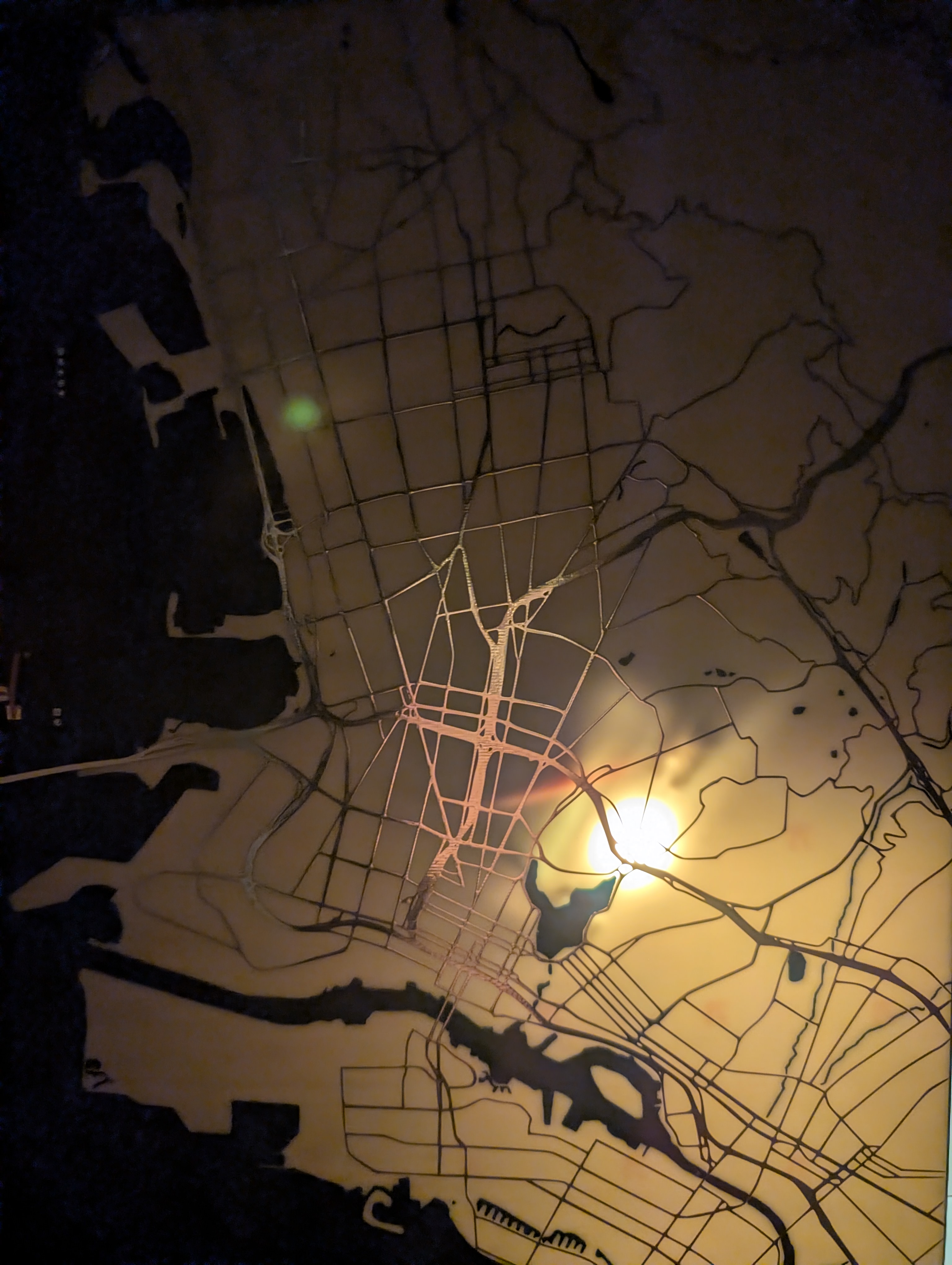
Since the minimum order for a custom PCB was 5, I had four extra boards to work with. They seemed like they’d make nice gifts as-is, but I still wanted to give them some basic functionality. Since I wasn’t expecting people to run a server to display locations, I came up with the idea of fitting the guts of a solar garden light onto a board so it would glow at night.
Full Application
This demo shows a simulated scenario where Joe is driving to Sue’s house. Once he arrives, the map alternates between them:
Here’s some samples of uploading background images to the display:
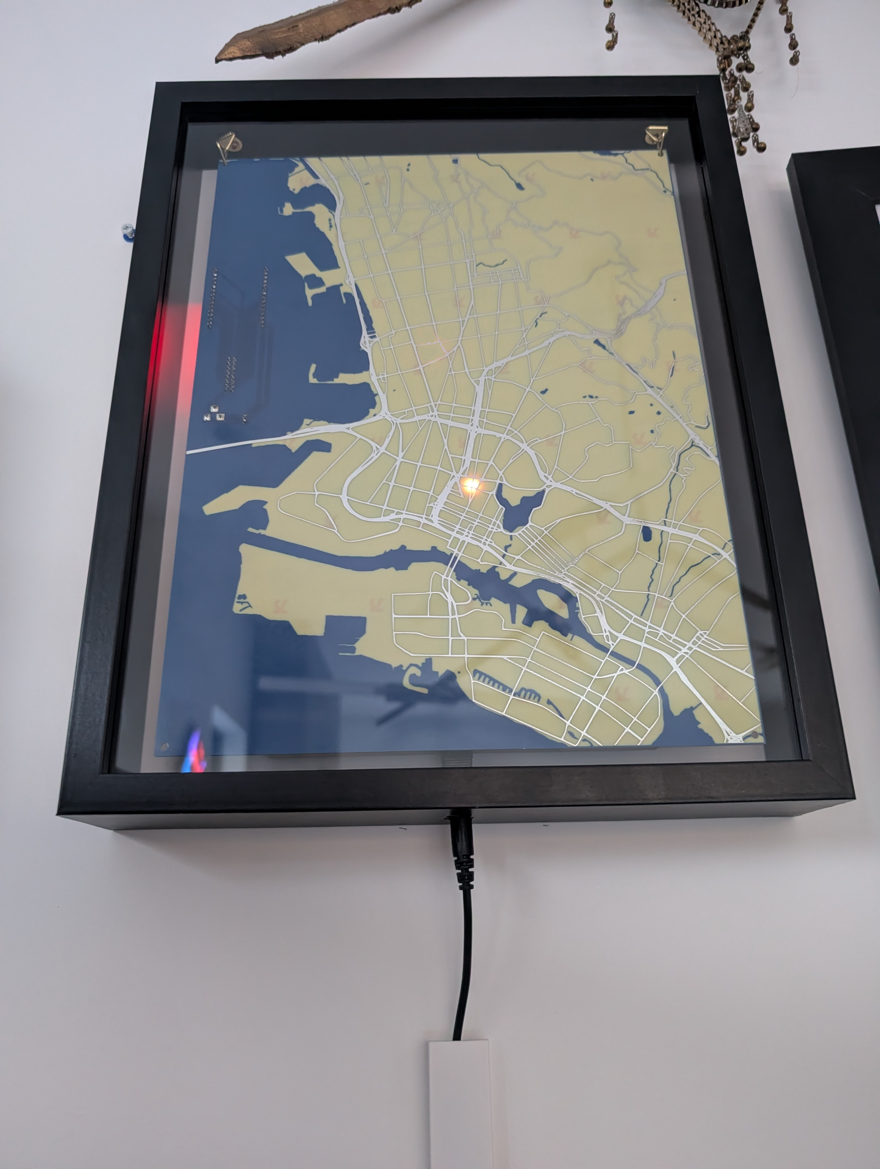
I ended up framing things to make it look classier:
In the end I got everything I wanted working, but in the next section I’ll go into some of the many improvements I could make.
All designs and code for this project can be found at: https://github.com/axlan/pcb-map
Improvements
Hardware
- Choose a more common ESP32/ESP8266 footprint - The particular board I had on hand was one I got from AliExpress years ago. Its pinout wasn’t very standardized. Since I’m using it on a printed board, it probably would have been worth targeting a better-documented dev board footprint.
- Select a thinner PCB - One of the PCBWay options I left at the default was board thickness. The lights are visible through the PCB, but they’re a little dimmer in daylight than I’d like. I think this would have been simply addressed by ordering a thinner board.
- Avoid blocking the ESP32 antenna - I laid out the connectors without much thought. In hindsight, I wouldn’t have placed the ESP32 on the back behind a solid copper layer. It still works, but the Wi-Fi signal strength is much worse than it could be, and it probably wouldn’t work at all if the device weren’t fairly close to the router.
- Avoid blocking the ESP32 USB - A similar mistake was placing the ESP32 too close to the LED matrix HUB75 connector. The USB and the display can’t be connected simultaneously since they block each other. I originally didn’t see this as a problem since I was planning on using a separate power connector, but once I was using the board I realized I could have used this port with data-only cables or high-power USB-C supplies.
- Add more silkscreen info - I didn’t include any useful silkscreen on the board. I should have at least labeled the orientation of each connector to make plugging them in easier.
Software
- Support special location indicators - This was an idea for better indicating when users are at known places like home or school. Originally I had thought I could shine LEDs under the “water” sections of the map with arrows pointing to their locations. Since the copper makes those sections opaque, I could instead add LEDs to the top of the board, or integrate them into the legend somehow.
- Add Event Indicators - In addition to showing the route to events, I could have some indicator that an event start time is coming.